Definition of a Logic Gate Diagram
A logic gate diagram is a visual representation of how different logic gates are connected in a digital circuit. Instead of describing logical operations with words or equations, the diagram uses standardized symbols and lines to show how signals flow between them. In short, a logic gate diagram acts as a blueprint for digital decision-making, showing how simple logic gates come together to form complex systems like adders, comparators, memory units, and processors.
Why Logic Gate Diagrams are Important
Logic gate diagrams play a crucial role in understanding and designing digital systems. They transform abstract Boolean logic into visual circuits, making it easier to see how inputs and outputs interact.
Clarity in Design: Logic gate diagrams simplify complex logical relationships by showing them as connected symbols. This makes it easier to visualize how signals flow through a circuit, spot redundancies, and identify potential design flaws early.
Foundation of Digital Systems: Every digital device, from the simplest calculator to advanced microprocessors is built on logic gates. Diagrams illustrate how these gates combine into larger systems, helping us understand the inner workings of memory units, processors, and controllers.
Learning Tool: For students and beginners, diagrams provide a bridge between theoretical concepts (like truth tables and Boolean algebra) and practical applications. They make abstract logic more concrete, supporting deeper comprehension of how circuits actually function.
Efficient Communication: Circuit diagrams act as a universal language for engineers, technicians, and educators. By using standardized symbols, they remove ambiguity, making it easy for teams across different fields and regions to share, review, and collaborate on circuit designs.
Problem Solving: By studying diagrams, designers can trace signal paths, predict outcomes, and detect errors before building hardware. This saves time and cost, as potential issues can be resolved in the design phase rather than during testing or production.
Components of a Logic Gate Diagram
A logic gate diagram isn’t just a collection of shapes and lines but a standardized way to represent how digital circuits function. Each diagram is made up of a few core components that work together to illustrate the flow of information.
Inputs: The signals that feed into the gate, usually represented by lines on the left side of a symbol. Inputs are binary values (0 or 1) and can come from switches, sensors, or other gates.
Outputs: The result produced by the gate, shown as a line leaving the right side of the symbol. Outputs also carry binary values and can serve as inputs to other gates, forming larger circuits. These intermediate outputs, which connect multiple gates together, allow complex logic functions to be built step by step.
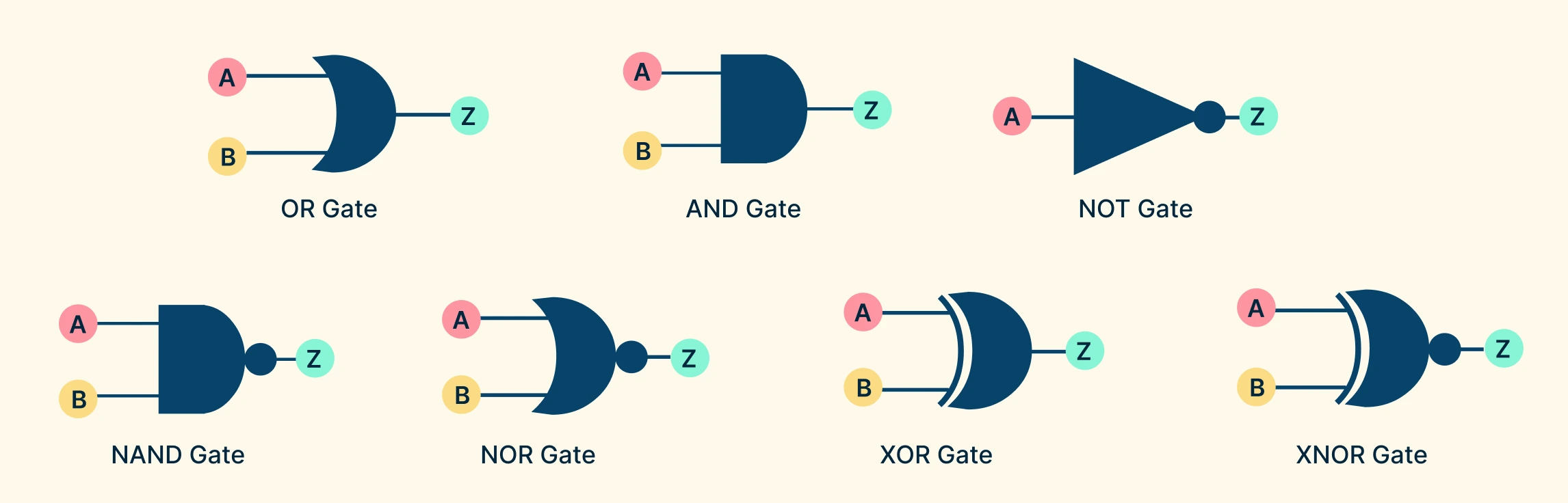
Logic Gate Symbols: Standardized shapes (such as the D-shape for AND, curved shape for OR, and triangle-with-bubble for NOT) that define which logical operation is being performed. These symbols make the diagram readable and universally understood.
Connecting Lines (Wires): Lines that connect inputs, outputs, and gates, representing the path of electrical signals. They show how different components interact in a circuit.
Labels/Variables: Letters or numbers (like A, B, C for inputs and Y, Z for outputs) are often added to clarify which signals are being used. This makes it easier to relate the diagram back to truth tables or Boolean expressions.
Combinations of Gates: Larger diagrams often combine multiple gates to show more complex behavior. For example, an XOR gate might be drawn as a combination of AND, OR, and NOT gates.
How to Read a Logic Gate Diagram
Reading a logic gate diagram means interpreting how inputs flow through gates to produce outputs. Once you understand the symbols and connections, it becomes like following a roadmap for digital logic.
Step 1: Identify Inputs and Logic Gate Symbols
Start at the left side of the diagram. Inputs are usually labeled (e.g., A, B, C) and represent binary signals (0 or 1). You will also need to identify the logic gates from their standard symbols. Each symbol tells you which logical operation is being performed. Read Logic Gate Types and Symbols to learn how to identify them.
Step 2: Follow the Signal Flow
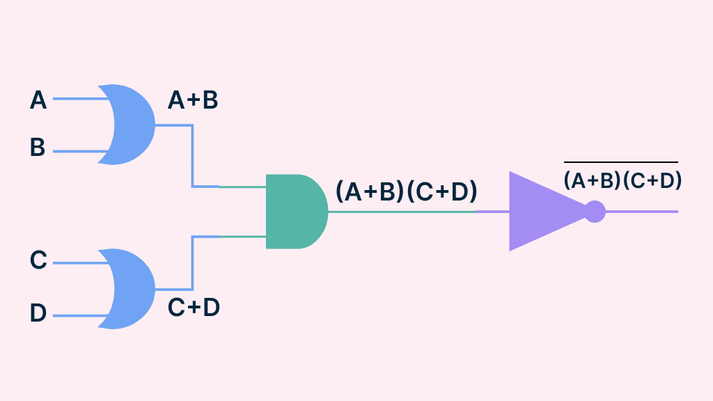
Trace the lines (wires) from inputs through each gate. Lines may split (fan-out) or combine, showing how signals interact.
Step 3: Apply the Logic Rule
At each gate, apply its rule to the inputs. Example: for an AND gate, output = 1 only if both inputs are 1. Be sure to check intermediate outputs in complex diagrams where gates may feed into other gates. Write down the result of each stage before moving to the next.
Step 4: Determine Final Output
Follow the flow until you reach the right side of the diagram. This is the overall output of the circuit.
Tip: Keep a truth table handy. For multi-input circuits, building a table of all possible input combinations makes it easier to predict outputs.
Why Use Creately for Drawing Logic Gate Diagrams
Ready-Made Logic Gate Symbols: Access a full library of standardized gate shapes (AND, OR, NOT, NAND, NOR, XOR, XNOR) that follow industry conventions.
Drag-and-Drop Simplicity: Quickly build circuits by dragging gates onto the canvas and connecting them with smart connectors that snap neatly into place.
Pre-Built Templates: Start faster with ready-to-use templates for common circuits. These templates can be customized, saving time for both beginners and advanced users.
Collaboration in Real Time: Work with your classmates, colleagues, or team members on the same diagram. You can share, comment, and edit together, making it ideal for group projects or engineering teams.
Customization and Styling: Change colors, labels, and layouts easily to make diagrams clearer for presentations, documentation, or teaching.
Integration with Other Tools: Export diagrams into formats like PNG, SVG, or PDF, or embed them directly into documents and presentations.
Real-World Applications of Logic Gate Diagrams
Logic gate diagrams model the circuits that power the devices and systems we use every day. By showing how gates connect and interact, these diagrams reveal the logic behind modern technology.
Computers and Processors: Every CPU, microprocessor, and GPU is built from millions of interconnected gates. Logic gate diagrams are used to design adders, multiplexers, and control circuits that handle instructions and perform calculations.
Memory and Storage Devices: Flip-flops, latches, and registers are the building blocks of RAM and storage controllers. These are designed using NAND and NOR gate diagrams. These allow devices to store and retrieve binary data reliably.
Digital Electronics and Consumer Devices: Everyday gadgets like calculators, digital watches, and remote controls are based on gate circuits. Designers use diagrams to map how inputs (button presses) turn into outputs (numbers on a screen, lights, or signals).
Control Systems: Logic diagrams drive automation in traffic lights, washing machines, elevators, and industrial machinery. They ensure that actions only occur when the right conditions are met.
Communication Systems: Gate diagrams help design circuits for error detection, encoding, and decoding which are critical for mobile phones, Wi-Fi, and satellite communication.
Security Systems: Burglar alarms, motion detectors, and digital locks rely on gate logic. For example, a door alarm may use an AND gate diagram to trigger only if both the door is open and the system is armed.
Free Circuit Diagram Examples Using Logic Gates


FAQs about Logic Gates Diagrams
Are logic gate diagrams used in real life or just for study?
Can I create and share logic gate diagrams online?
How do logic gate diagrams help in debugging digital circuits?
What are the common mistakes to avoid when drawing logic gate diagrams?
What are 7 logic gates used in logic gate diagrams?
Are logic gates used in AI?
Resources
Alvarado, Christine, and Michael Lazzareschi. “Properties of Real-World Digital Logic Diagrams.” First International Workshop on Pen-Based Learning Technologies (PLT 2007), May 2007, pp. 1–6, https://doi.org/10.1109/plt.2007.21.
Shenkman, S M. “Circuit Diagram Generation via Functional Logic.” Design Automation Conference, 25 June 1973, pp. 267–273, https://dl.acm.org/doi/abs/10.5555/800124.804026.